Semiconductor Manufacturing Processes

To offer the measuring solutions for
Semiconductor Manufacturing Processes
Measurement Solutions for Semiconductor Manufacturing Processes
The shift of production to electric vehicles, expansion of services promoted by commercialized 5G, and recovery of capital investment in data centers are all growing signs of recovery in the semiconductor market. The market is expected to show more growth and will be prepared for mass production to meet increasing demand. Mitutoyo, as a solution provider and metrology expert, is ready to provide measurement solutions for various semiconductor manufacturing processes.
Support & Development and Production of Semiconductor Manufacturing Processes
by Mitutoyo Measuring Equipments


Image licensed under ShutterStock.
A probe card is an interface that provides electrical and mechanical contact between the semiconductor wafer and the electronics test system. It is used for testing and validation of the circuits at the wafer level before proceeding to downstream processes such as dicing and bonding.
Quick Vision Apex Pro, a Vision Measuring Machine, provides a non-contact CNC measurement with high speed and accuracy. It is especially suitable for small parts like probe cards which require a detail inspection such as measurement of the pin height and hole diameter.
Featured Measuring Product:

Quick Vision Apex Pro
- Preventing nonconformities during mass production
- 3D measurement with multiple sensors
- Flaw Inspection Software DDPAK-QV

Image licensed under ShutterStock.
A lead frame is a thin layer of metal component that connects the wiring from tiny electrical terminals on the semiconductor surface to the large-scale circuitry on circuit boards. It is used to create integrated circuit packaging and is manufactured on assembly machines.
The measuring microscopes from Mitutoyo deliver the highest performance and accuracy in their class, enabling reduced part variation and measurement time. You can easily measure the width, pitch, height, twisting action, etc. of the lead frames.
Featured Measuring Product:

Measuring Microscope
- Ultra-wide View Field and High Magnification Observation
- Excellent usability, a high-NA and long working distance objectives enable effective observation
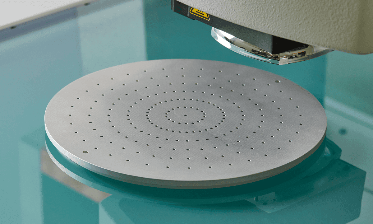
Showerheads are commonly used for even material deposition in semiconductor manufacturing. Their hole diameter, roundness and true position are important factors in determining uniformity of deposition.
As the semiconductor industry moves to processing at lower nanometer ranges, the margin for error gets smaller even as the opportunity for significant error grows. Clearly, these changes need to be accompanied by more stringent measurement and monitoring of the manufacturing process. Innovative new systems from Mitutoyo are now helping fabs achiever greater manufacturing consistency, reduce bottlenecks, improve productivity, reduce wafer scrap and ultimately maximize their return on investment.
Featured Measuring Product:

Quick Vision Pro Series with STREAM function
- Full automation – Continuous and high speed measurement during mass production.
- Preventing nonconformities during mass production.
- Unique STREAM function help to significantly reduce measurement cycle time.